● Integrated P-Channel Load Switch
● Input Voltage: 0.9 V to 3.6 V
● ON-Resistance (Typical Values)
● rON = 14 mΩ at VIN = 3.6 V
● rON = 20 mΩ at VIN = 2.5 V
● rON = 33 mΩ at VIN = 1.8 V
● rON = 67 mΩ at VIN = 1.2 V
● rON = 116 mΩ at VIN = 1.0 V
● 2-A Maximum Continuous Switch Current
● Quiescent Current:
● Typical 78 nA at 1.8 V
● Shutdown Current:
● Typical 35 nA at 1.8 V
● Low Threshold Control Input Enable the use of 1.2 V, 1.8 V, 2.5 V, or 3.3 V Logic
● Controlled Slew Rate to Avoid Inrush Currents
● tR = 30 µs at VIN = 1.8 V (TPS22921/2)
● tR = 200 µs at VIN = 1.8 V (TPS22922B)
● Quick Output Discharge (TPS22922/2B)
● ESD Performance Tested Per JESD 22
● 3000-V Human Body Model (A114-B, Class II)
● 1000-V Charged-Device Model (C101)
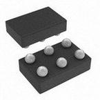
● Six Terminal Wafer-Chip-Scale DSBGA Package (nominal dimensions shown - see _Mechanical, Packaging, and Orderable Information_ for details)
● 0.9-mm × 1.4-mm, 0.5-mm Pitch, 0.5 mm Height (YZP)
● 0.9-mm × 1.4-mm, 0.5-mm Pitch, 0.625 mm Height (YZT)
● 0.8-mm × 1.2-mm, 0.4-mm Pitch, 0.5-mm Height (YFP)


