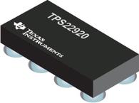
The TPS22920x is a small, space-saving load switch with controlled turn on to reduce inrush current. The device contains a N-channel MOSFET that can operate over an input voltage range of 0.75 V to 3.6 V and switch currents up to 4 A. An integrated charge pump biases the NMOS switch in order to achieve a minimum switch ON resistance (rON). The switch is controlled by an on/off input (ON), which is capable of interfacing directly with low-voltage control signals.
●The TPS22920x has a 1250-Ω on-chip resistor for quick output discharge when the switch is turned off which insures that the output is not left floating.
●The TPS22920x has an internally controlled rise time in order to reduce inrush current.
●The TPS22920x is available in an ultra-small, space- saving 8-pin CSP package and is characterized for operation over the free-air temperature range of 40°C to 85°C.
● Input Voltage Range: 0.75 V to 3.6 V
● Integrated Load Switch
● Integrated Pass-FET rDSON = 2 mΩ (Typ) at 3.6 V
● Typical ON-Resistance
● rON = 5.3 mΩ at VIN = 3.6 V
● rON = 5.4 mΩ at VIN = 2.5 V
● rON = 5.5 mΩ at VIN = 1.8 V
● rON = 5.8 mΩ at VIN = 1.2 V
● rON = 6.1 mΩ at VIN = 1.05 V
● rON = 7.3 mΩ at VIN = 0.75 V
● CSP-8 Package 0.9 mm × 1.9 mm, 0.5 mm Pitch
● 4-A Maximum Continuous Switch Current
● Shutdown Current 5.5-µA Max
● ON-Logic Available in Both Active High/Low:
● TPS22920 is Active High
● TPS22920L is Active Low
● Low Threshold Control Input
● Controlled Slew-Rate to Avoid Inrush Current
● Quick Output Discharge Resistor
● ESD Performance Tested Per JESD 22
● 4000-V Human-Body Model
●(A114-B, Class II)
● 1000-V Charged-Device Model (C101)


