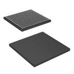
Part Datasheet Search > Digital Signal Processors(DSPs) > TI > TMS320C6748EZWTD4E Datasheet PDF
TMS320C6748EZWTD4E Datasheet PDF - TI
| Manufacturer: | TI |
| Category: | Digital Signal Processors(DSPs) |
| Case Package: | 361-LFBGA |
| Description: | DSP Fixed-Point/Floating-Point 32Bit/64Bit 456MHz 3648MIPS 361Pin NFBGA |
| Documentation: | TMS320C6748EZWTD4E User Reference Manual Guide (273 Pages) |
| Pictures: |
TMS320C6748EZWTD4E Datasheet PDF
ADatasheet has not yet included the datasheet for TMS320C6748EZWTD4E
If necessary, please send a supplementary document request to the administrator

TMS320C6748EZWTD4E Specifications
| TYPE | DESCRIPTION |
|---|---|
| Mounting Style | Surface Mount |
| Frequency | 375 GHz |
| Case/Package | 361-LFBGA |
| Clock Speed | 375 GHz |
| Number of UARTs | 3 UART |
TMS320C6748EZWTD4E Size & Package
| TYPE | DESCRIPTION |
|---|---|
| Product Lifecycle Status | Active |
| Packaging | Tray |
TMS320C6748EZWTD4E Environmental
TMS320C6748EZWTD4E Function Overview
The TMS320C6748 fixed- and floating-point DSP is a low-power applications processor based on a C674x DSP core. This DSP provides significantly lower power than other members of the TMS320C6000™ platform of DSPs.
●The device enables original-equipment manufacturers (OEMs) and original-design manufacturers (ODMs) to quickly bring to market devices with robust operating systems, rich user interfaces, and high processor performance through the maximum flexibility of a fully integrated, mixed processor solution.
●The device DSP core uses a 2-level cache-based architecture. The level 1 program cache (L1P) is a 32-KB direct mapped cache, and the level 1 data cache (L1D) is a 32-KB 2-way, set-associative cache. The level 2 program cache (L2P) consists of a 256-KB memory space that is shared between program and data space. L2 memory can be configured as mapped memory, cache, or combinations of the two. Although the DSP L2 is accessible by other hosts in the system, an additional 128KB of RAM shared memory is available for use by other hosts without affecting DSP performance.
●For security-enabled devices, TI’s Basic Secure Boot lets users protect proprietary intellectual property and prevents external entities from modifying user-developed algorithms. By starting from a hardware-based “root-of-trust," the secure boot flow ensures a known good starting point for code execution. By default, the JTAG port is locked down to prevent emulation and debug attacks; however, the JTAG port can be enabled during the secure boot process during application development. The boot modules are encrypted while sitting in external nonvolatile memory, such as flash or EEPROM, and are decrypted and authenticated when loaded during secure boot. Encryption and decryption protects customers’ IP and lets them securely set up the system and begin device operation with known, trusted code.
●Basic Secure Boot uses either SHA-1 or SHA-256, and AES-128 for boot image validation. Basic Secure Boot also uses AES-128 for boot image encryption. The secure boot flow employs a multilayer encryption scheme which not only protects the boot process but also offers the ability to securely upgrade boot and application software code. A 128-bit device-specific cipher key, known only to the device and generated using a NIST-800-22 certified random number generator, is used to protect customer encryption keys. When an update is needed, the customer uses the encryption keys to create a new encrypted image. Then the device can acquire the image through an external interface, such as Ethernet, and overwrite the existing code. For more details on the supported security features or TI’s Basic Secure Boot, see the .
●The peripheral set includes: a 10/100 Mbps Ethernet media access controller (EMAC) with a management data input/output (MDIO) module; one USB2.0 OTG interface; one USB1.1 OHCI interface; two I2C Bus interfaces; one multichannel audio serial port (McASP) with 16 serializers and FIFO buffers; two multichannel buffered serial ports (McBSPs) with FIFO buffers; two serial peripheral interfaces (SPIs) with multiple chip selects; four 64-bit general-purpose timers each configurable (one configurable as a watchdog); a configurable 16-bit host-port interface (HPI); up to 9 banks of general-purpose input/output (GPIO) pins, with each bank containing 16 pins with programmable interrupt and event generation modes, multiplexed with other peripherals; three UART interfaces (each with RTS and CTS); two enhanced high-resolution pulse width modulator (eHRPWM) peripherals; three 32-bit enhanced capture (eCAP) module peripherals which can be configured as 3 capture inputs or 3 APWM outputs; two external memory interfaces: an asynchronous and SDRAM external memory interface (EMIFA) for slower memories or peripherals; and a higher speed DDR2/Mobile DDR controller.
●The EMAC provides an efficient interface between the device and a network. The EMAC supports both 10Base-T and 100Base-TX, or 10 Mbps and 100 Mbps in either half- or full-duplex mode. Additionally, an MDIO interface is available for PHY configuration. The EMAC supports both MII and RMII interfaces.
●The Serial ATA (SATA) controller provides a high-speed interface to mass data storage devices. The SATA controller supports both SATA I (1.5 Gbps) and SATA II (3.0 Gbps).
●The Universal Parallel Port (uPP) provides a high-speed interface to many types of data converters, FPGAs, or other parallel devices. The uPP supports programmable data widths between 8- to 16-bits on both channels. Single-data rate and double-data rate transfers are supported as well as START, ENABLE, and WAIT signals to provide control for a variety of data converters.
●A video port interface (VPIF) provides a flexible video I/O port.
●The rich peripheral set provides the ability to control external peripheral devices and communicate with external processors. For details on each peripheral, see the related sections in this document and the associated peripheral reference guides.
●The device has a complete set of development tools for the DSP. These tools include C compilers, a DSP assembly optimizer to simplify programming and scheduling, and a Windows debugger interface for visibility into source code execution.
show more
TMS320C6748EZWTD4E Documents
Part Datasheet PDF Search
Example: STM32F103
72,405,303 Parts Datasheet PDF, Update more than 5,000 PDF files ervery day.

