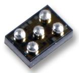
The SN74LVC2G125YZPR is a dual Bus Buffer Gate with 3-state outputs. The outputs are disabled when the associated output-enable (OE) input is high. To ensure the high-impedance state during power up or power down, OE should be tied to VCC through a pull-up resistor, the minimum value of the resistor is determined by the current-sinking capability of the driver. This device is fully specified for partial-power-down applications using Ioff. The Ioff circuitry disables the outputs, preventing damaging current backflow through the device when it is powered down.
● ±24mA Output drive at 3.3V
● <0.8V at VCC = 3.3V (typical) VOLP (Output ground bounce)
● >2V at VCC = 3.3V Typical VOHV (Output VOH undershoot)
● Inputs from a Maximum of 5.5V down
● 10µA Maximum ICC low power consumption
● Maximum tpd of 4.3ns at 3.3V
● Ioff supports live insertion, partial power down mode and back drive protection
● ESD protection exceeds JESD 22
● Latch-up performance exceeds 100mA per JESD 78, Class II


