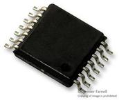
The SN74LVC125APWR is a quadruple Bus Buffer Gate designed for 1.65 to 3.6V VCC operation. The SN74LVC125A device feature independent line drivers with 3-state outputs. Each output is disabled when the associated output-enable (OE) input is high. To ensure the high-impedance state during power up or power down, OE should be tied to VCC through a pull-up resistor, the minimum value of the resistor is determined by the current-sinking capability of the driver. Inputs can be driven from either 3.3 or 5V devices. This feature allows the use of this device as a translator in a mixed 3.3/5V system environment. It is suitable for cable modem termination systems, point-to-point microwave backhaul, private branch exchanges (PBX), vector signal analyzers and generators.
● Separate OE for all 4 buffers
● Inputs accept voltage to 5.5V
● Maximum tpd of 4.8ns at 3.3V
● Latch-up performance exceeds 250mA per JESD 17
● ±50mA Continuous output current
● ±100mA Continuous current through VCC or GND
●ESD sensitive device, take proper precaution while handling the device.


