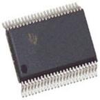
The SN74CB3Q16210 is a high-bandwidth FET bus switch utilizing a charge pump to elevate the gate voltage of the pass transistor, providing a low and flat ON-state resistance (ron). The low and flat ON-state resistance allows for minimal propagation delay and supports rail-to-rail switching on the data input/output (I/O) ports. The device also features low data I/O capacitance to minimize capacitive loading and signal distortion on the data bus. Specifically designed to support high-bandwidth applications, the SN74CB3Q16210 provides an optimized interface solution ideally suited for broadband communications, networking, and data-intensive computing systems.
●The SN74CB3Q16210 is organized as two 10-bit bus switches with separate output-enable (1OE\, 2OE\\\\) inputs. It can be used as two 10-bit bus switches or as one 20-bit bus switch. When OE\ is low, the associated 10-bit bus switch is ON and the A port is connected to the B port, allowing bidirectional data flow between ports. When OE\ is high, the associated 10-bit bus switch is OFF, and a high-impedance state exists between the A and B ports.
●This device is fully specified for partial-power-down applications using Ioff. The Ioff circuitry prevents damaging current backflow through the device when it is powered down. The device has isolation during power off.
●To ensure the high-impedance state during power up or power down, OE\ should be tied to VCC through a pullup resistor; the minimum value of the resistor is determined by the current-sinking capability of the driver.


