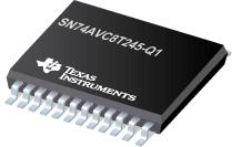
The SN74AVC8T245-Q1 is an 8-bit noninverting bus transceiver that uses two separate configurable power-supply rails. The SN74AVC8T245-Q1 operation is optimimal with VCCA and VCCB set at
●1.4 V to 3.6 V. It is operational with VCCA and VCCB as low as 1.2 V. The A port is designed to track VCCA. VCCA accepts any supply voltage from 1.2 V to 3.6 V. The B port is designed to track VCCB. VCCB accepts any supply voltage from 1.2 V to 3.6 V. This allows for universal low-voltage bidirectional translation between any of the 1.2-V, 1.5-V, 1.8-V, 2.5-V, and 3.3-V voltage nodes.
●The SN74AVC8T245 design enables asynchronous communication between data buses. The device transmits data from the A bus to the B bus or from the B bus to the A bus, depending on the logic level at the direction-control (DIR) input. One can use the output-enable (OE) input to disable the outputs so the buses are effectively isolated.
●In the SN74AVC8T245 design, VCCA supplies the control pins (DIR and OE).
●This device specification covers partial-power-down applications using Ioff. The Ioff circuitry disables the outputs, preventing damaging current backflow through a powered-down device.
●The VCC isolation feature ensures that if either VCC input is at GND, both ports are in the high-impedance state.
●To ensure the high-impedance state during power up or power down, tie OE to VCC through a pullup resistor; the current-sinking capability of the driver determines the minimum value of the resistor.
● Qualified for Automotive Applications
● AEC Q100 Test Guidance With the Following
●Results:
● Device Temperature Grade 1: 40°C to 125°C
●Ambient Operating Temperature Range
● Device HBM ESD Classification Level H2
● Device CDM ESD Classification Level C3B
● Control Inputs VIH and VIL Levels Are Referenced
●to VCCA Voltage
● VCC Isolation Feature If Either VCC Input Is at
●GND, All I/O Ports Are in the High-Impedance
●State
● Ioff Supports Partial Power-Down-Mode Operation
● Fully Configurable Dual-Rail Design Allows Each
●Port to Operate Over the Full 1.4-V to 3.6-V
●Power-Supply Range
● I/Os Are 4.6-V Tolerant
● Maximum Data Rates
● 170 Mbps (VCCA < 1.8 V or VCCB < 1.8 V)
● 320 Mbps (VCCA ≥ 1.8 V and VCCB ≥ 1.8 V)
● Latch-Up Performance Exceeds 100 mA per
●JESD 78, Class II


