2.5V / 3.3V Dual Channel Programmable Clock/Data Delay with Differential CML Outputs
●Multi−Level Inputs w/ Internal Termination
●The NB6L295 is a Dual Channel Programmable Delay Chip designed primarily for Clock or Data de−skewing and timing
●adjustment. The NB6L295 is versatile in that two individual variable delay channels, PD0 and PD1, can be configured in one of two operating modes, a Dual Delay or an Extended Delay.
●•Input Clock Frequency > 1.5 GHz with 550 mV VOUTPP
●•Input Data Rate > 2.5 Gb/s
●•Programmable Delay Range: 0 ns to 6 ns per Delay Channel
●•Programmable Delay Range: 0 ns to 11.2 ns for Extended Delay Mode
●•Total Delay Range: 3.2 ns to 8.8 ns per Delay Channel
●•Total Delay Range: 6 ns to 17 ns in Extended Delay Mode
●•Monotonic Delay: 11 ps Increments in 511 Steps
●•Linearity 20 ps, Maximum
●•100 ps Typical Rise and Fall Times
●•3 ps Typical Clock Jitter, RMS
●•20 ps Pk−Pk Typical Data Dependent Jitter
●•LVPECL, CML or LVDS Differential Input Compatible
●•LVPECL, LVCMOS, LVTTL Single−Ended Input Compatible
●•3−Wire Serial Interface
●•Operating Range: VCC= 2.375 V to 3.6 V
●•LVPECL Output Level; 780 mV Peak−to−Peak, Typical
●•Internal 50 Input Termination Provided
●•−40°C to 85°C Ambient Operating Temperature
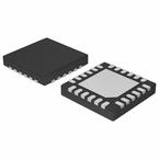
●•24−Pin QFN, 4 mm x 4 mm
●•These are Pb−Free Devices


