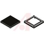
| TYPE | DESCRIPTION |
|---|
| Mounting Style | Surface Mount |
| Frequency | 700 MHz |
| Number of Pins | 32 Pin |
| Supply Voltage (DC) | 2.38 V (min) |
| Case/Package | QFN |
| Halogen Free Status | Halogen Free |
| Supply Current | 70.0 mA |
| TYPE | DESCRIPTION |
|---|
| Product Lifecycle Status | Active |
| Packaging | Tube |
The NB4L339 is a multi-function Clock generator featuring a 2:1 Clock multiplexer front end and simultaneously outputs a selection of four different divide ratios from its four divider blocks; div1, div2, div4 and div8. One divide block has a choice of div1 or div2. The output of each divider block is fanned-out to two identical differential LVPECL copies of the selected clock. All outputs provide standard LVPECL voltage levels when externally terminated with a 50-ohm resistor to VCC - 2 V. The differential Clock inputs incorporate internal 50-ohm termination resistors and will accept LVPECL, CML or LVDS logic levels. The common Output Enable pin (EN) is synchronous so that the internal dividers will only be enabled/disabled when the internal clock is in the LOW state. This avoids any chance of generating a runt clock pulse on the internal clock when the device is enabled/disabled as can happen with an asynchronous control. An internal runt pulse could lead to losing synchronization between the internal divider stages. The internal enable flip-flop is clocked on the falling edge of the input clock. Therefore, all associated specification limits are referenced to the negative edge of the clock input. This device is housed in a 5x5 mm 32 pin QFN package.
●Features | | Benefits
●---|---|---
● | | | | |
● 0.5 ps Typical RMS Random Clock Period Jitter
●| |
● Very Low Jitter Clock Output
● LVPECL, CML or LVDS Input Compatible
●| |
● Multi Level Input Interface
● 0.15 ps Typical RMS Phase Jitter
●| |
● Low Skew LVPECL Outputs, 15 ps typical
●| |
ON Semiconductor
12 Pages / 0.13 MByte
Part Datasheet PDF Search
72,405,303 Parts Datasheet PDF, Update more than 5,000 PDF files ervery day.


