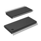
| TYPE | DESCRIPTION |
|---|
| Number of Pins | 56 Pin |
| Supply Voltage (DC) | 3.00 V (min) |
| Case/Package | TSSOP |
| Supply Current | 81.0 mA |
| Data Rate | 1.85 Gbps |
| Power Consumption | 258 W |
| TYPE | DESCRIPTION |
|---|
| Product Lifecycle Status | Active |
| Packaging | Rail |
The DS90CR286AMTD is a 3.3V Rising Edge Data Strobe LVDS Receiver converts the four LVDS data streams back into parallel 28-bits of LVCMOS data. The output of the receiver strobes on the rising edge. The receiver LVDS clock operates at rates from 20 to 66MHz. The device phase-locks to the input clock, samples the serial bit streams at the LVDS data lines and converts them into parallel output data. At an incoming clock rate of 66MHz, each LVDS input line is running at a bit rate of 462Mbps, resulting in a maximum throughput of 1.848Gbps. This device is an enhanced over prior generation receivers and provide a wider data valid time on the receiver output.
● Best-in-class set and hold times on RxOUTPUTs
● PLL requires no external components
● Compatible with TIA/EIA-644 LVDS standard
● <200µW Maximum Rx power-down mode
● 50% Duty cycle on receiver output clock
National
+3.3V Rising Edge Data Strobe LVDS 28Bit Channel Link-66MHz
TI
+3.3V Rising Edge Data Strobe LVDS 28Bit Channel - 66MHz 56-TSSOP
TI
+3.3V Rising Edge Data Strobe LVDS Receiver 28Bit Channel Link - 66MHz 56-TSSOP -40℃ to 85℃
TI
+3.3V Rising Edge Data Strobe LVDS Receiver 28Bit Channel Link - 66MHz 56-TSSOP -40℃ to 85℃
National Semiconductor
LVDS Receiver 56Pin TSSOP Rail
TI
+3.3V Rising Edge Data Strobe LVDS Receiver 28Bit Channel Link - 66MHz 56-TSSOP -40℃ to 85℃
TI
TEXAS INSTRUMENTS DS90CR286MTD/NOPB LVDS Driver, Receiver, 250 ps, 105mA, -40℃, 85℃, 3V
TI
LVDS Receiver 0.45V 56Pin TSSOP Tube
TI
LVDS Receiver 462Mbps 3.3V 56Pin TSSOP T/R
TI
TEXAS INSTRUMENTS DS90CR286ATDGGRQ1 LVDS Driver, LVDS Receiver, 1.8μA, -40℃, 105℃, 3V
Part Datasheet PDF Search
72,405,303 Parts Datasheet PDF, Update more than 5,000 PDF files ervery day.


