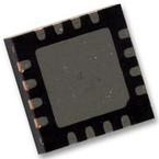
The CDCLVD2102RGTT is a Clock Buffer distributes two clock inputs (IN0, IN1) to a total of 4 pairs of differential LVDS clock outputs (OUT0, OUT3). Each buffer block consists of one input and 2 LVDS outputs. The inputs can either be LVDS, LVPECL or LVCMOS. It is specifically designed for driving 50R transmission lines. If driving the inputs in single ended mode, the appropriate bias voltage (VAC_REF) should be applied to the unused negative input pin. Using the control pin (EN), outputs can be either disabled or enabled. If the EN pin is left open two buffers with all outputs are enabled, if switched to a logical 0 both buffers with all outputs are disabled (static logical 0), if switched to a logical 1, one buffer with two outputs is disabled and another buffer with two outputs is enabled. The part supports a fail-safe function. It incorporates an input hysteresis, which prevents random oscillation of the outputs in absence of an input signal.
● 1:2 Differential buffer
● Universal inputs accept LVDS, LVPECL and LVCMOS
● One input dedicated for two outputs
● 4 LVDS outputs, ANSI EAI/TIA-644A standard compatible
● <300fs RMS in 10kHz to 20MHz low additive jitter
● 15ps Maximum low output skew
● Green product and no Sb/Br
●Device has limited built-in ESD protection. The leads should be shorted together or the device placed in conductive foam during storage or handling to prevent electrostatic damage to the MOS gates.


