| TYPE | DESCRIPTION |
|---|
| Mounting Style | Surface Mount |
| Frequency | 60.0 MHz |
| Number of Pins | 20 Pin |
| Supply Voltage (DC) | 5.00 V |
| Case/Package | 5V |
| Number of Outputs | 8 Output |
| Supply Current | 8.00 µA |
| Clock Speed | 60.0 MHz |
| Output Current Drive | -1.00 mA |
| TYPE | DESCRIPTION |
|---|
| Product Lifecycle Status | Active |
| Packaging | Tube |
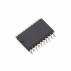
The CDC208 contains dual clock-driver circuits that fanout one input signal to four outputs with minimum skew for clock distribution (see Figure 2). The device also offers two output-enable (OE1\ and OE2\\\\) inputs for each circuit that can force the outputs to be disabled to a high-impedance state or to a high- or low-logic level independent of the signal on the respective A input.
●Skew parameters are specified for a reduced temperature and voltage range common to many applications.
●The CDC208 is characterized for operation from -40°C to 85°C.
TI
5V Dual 1-to-4 clock driver
TI
Clock Fanout Buffer 8Out 2IN 1:4 20Pin SOIC Tube
TI
Clock Fanout Buffer 8Out 2IN 1:4 20Pin SOP T/R
TI
5V Dual 1-to-4 clock driver 20-SO -40℃ to 85℃
TI
Clock Fanout Buffer 8Out 2IN 1:4 20Pin SOIC T/R
TI
Clock Fanout Buffer 8Out 2IN 1:4 20Pin SOIC Tube
TI
Clock Fanout Buffer 8Out 2IN 1:4 20Pin SOIC T/R
TI
Clock Fanout Buffer 8Out 2IN 1:4 20Pin SOP Tube
TI
Clock Fanout Buffer 8Out 2IN 1:4 20Pin SOP T/R
TI
Clock Fanout Buffer 8Out 20Pin PDIP
Part Datasheet PDF Search
72,405,303 Parts Datasheet PDF, Update more than 5,000 PDF files ervery day.


