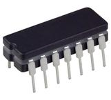
| TYPE | DESCRIPTION |
|---|
| Mounting Style | Through Hole |
| Case/Package | CDIP |
| Number of Bits | 6 Bit |
| Voltage Nodes | 5.00 V, 10.0 V, 15.0 V |
| TYPE | DESCRIPTION |
|---|
| Product Lifecycle Status | Active |
| Packaging | Tube |
3 Description
●The CD4069UB device consist of six CMOS inverter circuits. These devices are intended for all general purpose inverter applications where the medium power TTL-drive and logic-level-conversion capabilities of circuits such as the CD4009 and CD4049 hex inverter and buffers are not required.
●Features
●• Standardized Symmetrical Output Characteristics
●• Medium Speed Operation: –tPHL, tPLH = 30 ns at 10 V (Typical)
●• 100% Tested for Quiescent Current at 20 V
●• Maximum Input Current of 1 µA at 18 V Over Full Package-Temperature Range, 100 nA at 18 V and 25°C
●• Meets All Requirements of JEDEC Tentative Standard No. 13B, Standard Specifications for Description of B Series CMOS Devices
●Applications
●• Logic Inversion
●• Pulse Shaping
●• Oscillators
●• High-Input-Impedance Amplifiers
Part Datasheet PDF Search
72,405,303 Parts Datasheet PDF, Update more than 5,000 PDF files ervery day.


