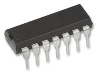
| TYPE | DESCRIPTION |
|---|
| Mounting Style | Through Hole |
| Number of Pins | 14 Pin |
| Supply Voltage (DC) | 3.00 V to 18.0 V |
| Case/Package | DIP |
| Output Current | 6.80 mA |
| Number of Circuits | 2 Circuit |
| Number of Bits | 2 Bit |
| Propagation Delay Max (tpd) | 250 ns |
| Voltage Nodes | 5.00 V, 10.0 V, 15.0 V |
| Quiescent Current | 20.0 nA |
| Number of Gates | 2 Gate |
| Input Capacitance | 5.00 pF |
| Output Current Drive | -1.00 mA |
| TYPE | DESCRIPTION |
|---|
| Product Lifecycle Status | Active |
| Packaging | Tube |
The CD4012BE is a CMOS dual 4-input NAND Gate provide the system designer with direct implementation of the NAND function and supplement the existing family of CMOS gates. All inputs and outputs are buffered. Meets all requirements of JEDEC tentative standard no. 13B, "standard specifications for description of "B" series CMOS devices".
● Propagation delay time = 60ns (typ.) at CL = 50pF, VDD = 10V
● Buffered inputs and outputs
● Standardized symmetrical output characteristics
● Maximum input current of 1µA at 18V
● 100% Tested for quiescent current at 20V
TI
NAND Gate 2Element 4IN CMOS 14Pin PDIP Tube
TI
NAND Gate 2Element 4IN CMOS 14Pin SOIC T/R
TI
NAND Gate 2Element 4IN CMOS 14Pin TSSOP T/R
TI
NAND Gate 2Element 4IN CMOS 14Pin SOP T/R
TI
NAND Gate 2Element 4IN CMOS 14Pin SOP T/R
TI
NAND Gate 2Element 4IN CMOS 14Pin SOIC Tube
TI
NAND Gate 2Element 4IN CMOS 14Pin SOIC Tube
TI
NAND Gate 2Element 4IN CMOS 14Pin CDIP Tube
TI
NAND Gate 2Element 4IN CMOS 14Pin PDIP Tube
TI
NAND Gate 2Element 4IN CMOS 14Pin SOIC T/R
Part Datasheet PDF Search
72,405,303 Parts Datasheet PDF, Update more than 5,000 PDF files ervery day.


