Product Details
●The ADCLK854 is a 1.2 GHz/250 MHz LVDS/CMOS fanout buffer optimized for low jitter and low power operation. Possible configurations range from 12 LVDS to 24 CMOS outputs, including combinations of LVDS and CMOS outputs. Three control lines are used to determine whether fixed blocks of outputs (three banks of four) are LVDS or CMOS outputs.
●The ADCLK854 offers two selectable inputs and a sleep mode feature. The IN_SEL pin state determines which input is fanned out to all the outputs. The SLEEP pin enables a sleep mode to power down the device.
●The inputs accept various types of single-ended and differential logic levels including LVPECL, LVDS, HSTL, CML, and CMOS. Table 8 provides interface options for each type of connection.
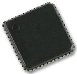
●This device is available in a 48-pin LFCSP package. It is specified for operation over the standard industrial temperature range of −40°C to +85°C.
●### Features and Benefits
● 2 selectable differential inputs
● Selectable LVDS/CMOS outputs
● Up to 12 LVDS (1.2 GHz) or 24 CMOS (250 MHz) outputs
● <12 mW per channel (100 MHz operation)
● 54 fs rms integrated jitter (12 kHz to 20 MHz)
● 100 fs rms additive broadband jitter
●|
● 2.0 ns propagation delay (LVDS)
● 135 ps output rise/fall (LVDS)
● 70 ps output-to-output skew (LVDS)
● Sleep mode
● Pin programmable control
● 1.8 V power supply
●---|---


