| TYPE | DESCRIPTION |
|---|
| Mounting Style | Surface Mount |
| Frequency | 1.20 GHz |
| Number of Pins | 24 Pin |
| Supply Voltage (DC) | 1.71 V (min) |
| Case/Package | LFCSP |
| Number of Outputs | 6 Output |
| TYPE | DESCRIPTION |
|---|
| Product Lifecycle Status | Active |
| Packaging | Tray |
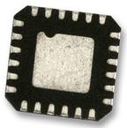
The ADCLK846BCPZ is a 12-output low-power clock Fan-out Buffer optimized for low jitter and low power operation. Possible configurations range from 6 LVDS to 12 CMOS outputs, including combinations of LVDS and CMOS outputs. Two control lines are used to determine whether fixed blocks of outputs are LVDS or CMOS outputs. The clock input accepts various types of single-ended and differential logic levels including LVPECL, LVDS, HSTL, CML and CMOS.
● Pin-programmable control
● Sleep mode
● 54fs Integrated jitter (12kHz to 20MHz)
● 100fs Additive broadband jitter
● 2ns Propagation delay (LVDS)
● 135ps Output rise/fall (LVDS)
● 65ps Output-to-output skew (LVDS)
ADI
1.8V, 6 LVDS/12 CMOS Outputs Low Power Clock Fanout Buffer
ADI
Clock Fanout Buffer 6Out 1IN 1:6 24Pin LFCSP EP Tray
ADI
Clock Fanout Buffer 6Out 1IN 1:6 24Pin LFCSP EP T/R
ADI
Evaluation Board For 1.8V, 6 LVDS/12 CMOS OutPuts Low Power Clock Fan-Out Buffer
Part Datasheet PDF Search
72,405,303 Parts Datasheet PDF, Update more than 5,000 PDF files ervery day.


