Product Details
●The AD7625 is a 16-bit, 6 MSPS, charge redistribution successive approximation register (SAR) based architecture analog-to-digital converter (ADC). SAR architecture allows unmatched perfor-mance both in noise (93 dB SNR) and in linearity (1 LSB). The AD7625 contains a high speed, 16-bit sampling ADC, an internal conversion clock, and an internal buffered reference. On the CNV± rising edge, it samples the voltage difference between the IN+ and IN− pins. The voltages on these pins swing in opposite phase between 0 V and REF. The 4.096 V reference voltage, REF, can be generated internally or applied externally.
●All converted results are available on a single LVDS self-clocked or echoed-clock serial interface, reducing external hardware connections.
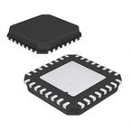
●The AD7625 is housed in a 32-lead, 5 mm × 5 mm LFCSP with operation specified from −40°C to +85°C.
●Applications
● High dynamic range telecommunications
● Receivers
● Digital imaging systems
● High speed data acquisition
● Spectrum analysis
● Test equipment
●### Features and Benefits
● Throughput: 6 MSPS
● SNR: 93 dB
● INL: ±0.45 LSB typical, ±1 LSB maximum
● DNL: ±0.3 LSB typical, ±0.5 LSB maximum
● Power dissipation: 135 mW
● 32-lead LFCSP (5 mm × 5 mm)
● SAR architecture
● No latency/no pipeline delay
● 16-bit resolution with no missing codes
● Please see data sheet for additional features