
Part Datasheet Search > Digital to Analog > ADI > AD667JP Datasheet PDF
AD667JP Datasheet PDF - ADI
| Manufacturer: | ADI |
| Category: | Digital to Analog |
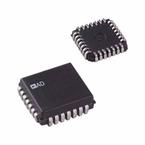
| Case Package: | PLCC |
| Description: | DAC 1CH Current Steering 12Bit 28Pin PLCC Tube |
| Documentation: | AD667JP Datasheet (8 Pages) |
| Pictures: |
AD667JP Datasheet PDF
ADatasheet has not yet included the datasheet for AD667JP
If necessary, please send a supplementary document request to the administrator

AD667JP Specifications
| TYPE | DESCRIPTION |
|---|---|
| Mounting Style | Surface Mount |
| Number of Pins | 28 Pin |
| Case/Package | PLCC |
| Number of Bits | 12 Bit |
| Power Dissipation | 555 mW |
| Resolution (Bits) | 12.0 Bit |
AD667JP Size & Package
| TYPE | DESCRIPTION |
|---|---|
| Product Lifecycle Status | Active |
| Packaging | Bulk, Tray |
AD667JP Environmental
AD667JP Function Overview
Product Details
●The AD667 is a complete voltage output 12-bit digital-to-analog converter including a high stability buried Zener voltage reference and double-buffered input latch on a single chip. The converter uses 12 precision high speed bipolar current steering switches and a laser trimmed thin-film resistor network to provide fast settling time and high accuracy.
●Microprocessor compatibility is achieved by the on-chip double-buffered latch. The design of the input latch allows direct interface to 4-, 8-, 12-, or 16-bit buses. The 12 bits of data from the first rank of latches can then be transferred to the second rank, avoiding generation of spurious analog output values. The latch responds to strobe pulses as short as 100 ns, allowing use with the fastest available microprocessors.
●The functional completeness and high performance in the AD667 results from a combination of advanced switch design, high speed bipolar manufacturing process, and the proven laser wafer-trimming (LWT) technology. The AD667 is trimmed at the wafer level and is specified to ±1/4 LSB maximum linearity error (K, B grades) at +25°C and ±1/2 LSB over the full operating temperature range.
●The subsurface (buried) Zener diode on the chip provides a low noise voltage reference which has long-term stability and temperature drift characteristics comparable to the best discrete reference diodes. The laser trimming process which provides the excellent linearity, is also used to trim the absolute value of the reference as well as its temperature coefficient. The AD667 is thus well suited for wide temperature range performance with ±1/2 LSB maximum linearity error and guaranteed monotonicity over the full temperature range. Typical full-scale gain TC is 5 ppm/°C.
●The AD667 is available in five performance grades. The AD667J and K are specified for use over the 0°C to +70°C temperature range and are available in a 28-pin molded plastic DIP (N) or PLCC (P) package. The AD667S grade is specified for the -55°C to +125°C range and is available in the ceramic DIP (D) or LCC (E) package. The AD667A and B are specified for use over the -25°C to +85°C temperature range and are available in a 28-pin hermetically sealed ceramic DIP (D) package.
●### Features and Benefits
● Complete 12-Bit D/A Function
●Double-Buffered Latch
●On Chip Output Amplifier
●High Stability Buried Zener Reference
● Single Chip Construction
● Monotonicity Guaranteed Over Temperature
● Linearity Guaranteed Over Temperature: 1/2 LSB max
● Settling Time: 3 µs max to 0.01%
● Guaranteed for Operation with ±12 V or ±15 V Supplies
● Low Power: 300 mW including Reference
● TTL/5 V CMOS Compatible Logic Inputs
● Low Logic Input Currents
● MIL-STD-883 Compliant Versions Available
show more
AD667JP Documents
AD667 Documents
ADI
ANALOG DEVICES AD667JNZ Digital to Analog Converter, 12Bit, 500KSPS, Parallel, ± 11.4V to ± 16.5V, DIP, 28Pins
ADI
ANALOG DEVICES AD667JPZ Digital to Analog Converter, 12Bit, Parallel, ± 11.4V to ± 16.5V, LCC, 28Pins
ADI
ANALOG DEVICES AD667SD Digital to Analog Converter, 12Bit, 500KSPS, ± 11.4V to ± 16.5V, DIP, 28Pins
Part Datasheet PDF Search
Example: STM32F103
72,405,303 Parts Datasheet PDF, Update more than 5,000 PDF files ervery day.